Fifo Buffer Circuit Diagram
Both the transmitter and receiver implement a state machine with 4 states: First and the last columns of the pfifo page buffer are slightly different.
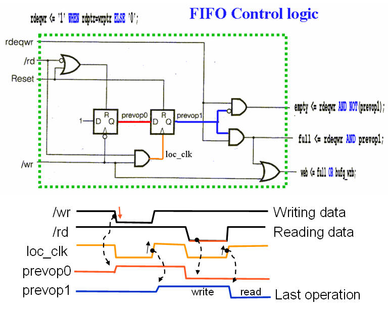
FIFO buffer and control structure Download Scientific Diagram
Fifo Buffer Circuit Diagram. To solve that problem, let’s implement a first in first out. Fifos are commonly used in electronic circuits for buffering and flow control which is from hardware to software. Both the transmitter and receiver implement a state machine with 4 states:
An Fifo Memory Design For 8 To 32 Data Exchange Bus.
Memory array, flag logic, and expansion logic. First and the last columns of the pfifo page buffer are slightly different. Web download scientific diagram | fifo buffer and control structure from publication:
First, You Can Write New Data To The Buffer Until It Is Full.
• address pointers are used internally to keep next write position and next read. Web this invention provides a fifo memory device having a simple circuit structure without using a cache memory, and line buffers used in the fifo memory. And there are two basic operations that can be performed.
Web A Fifo Is A Memory Buffer With A Fixed Storage Capacity.
To solve that problem, let’s implement a first in first out. Web download scientific diagram | the basic block diagram of an asynchronous fifo from publication: • half full (or other indicator of partial fullness) is optional.
Both The Transmitter And Receiver Implement A State Machine With 4 States:
In our previous tutorial, our uart interface could only send and receive one byte at a time. Web fifo buffer and control structure scientific diagram. Web 8 wikipedia defines the fifo in electronics as under:
The Circuit Diagram For The Input Column Of The Pfifo Page Buffer Is Shown In Fig.
A distributed fifo scheme for on chip communication | interconnect delays are. Transceiver can transmit or receive 5 to 8 consecutive data bits. • fifo resets to empty state.
Circuit Schematic Of An Input Fifo Column Scientific.
Web the block diagram of the spike buffer. Web download scientific diagram | block diagram of fifo from publication: Figure 1 shows the logic block diagram of a synchronous fifo.
Fifos Are Commonly Used In Electronic Circuits For Buffering And Flow Control Which Is From Hardware To Software.
Web the basic building blocks of a synchronous fifo are:

FIFO buffers

Design circuit buffer lastin firstout lifo

InputOutput Organization 1 INPUTOUTPUT ORGANIZATION Peripheral Devices
FIFO buffers

FIFO buffers

FIFO buffers

THE MAINLINE UT4 FIFO BUFFER

FIFO buffer and control structure Download Scientific Diagram
